


All Products
-
 DavidGood company with nice service and high quality and high reputation. One of our reliable supplier , goods are delivered in time and nice package.
 -
 John MorrisMaterial experts, rigorous processing, timely discovery of problems in design drawings and communication with us, thoughtful service, reasonable price and good quality, I believe we will have more cooperation.
 -
 JorgeThank you for your good after-sales service. Excellent expertise and technical support helped me a lot.
 -
 PetraThrough very good communication all problems solved, satisfied with my purchase
 -
 Adrian HayterThe goods purchased this time are very satisfied, the quality is very good, and the surface treatment is very good. I believe we will order the next order soon.
20mm Molybdenum Sputtering Targets For The Semiconductor Industry Molybdenum Target Molybdenum Disc molybdenum products


Product Details
| Name | Molybdenum Sputtering Targets For The Semiconductor Industry | Material | Molybdenum And Molybdenum Alloy |
|---|---|---|---|
| Purity | 99.95% | Density | 10.2g/cm3 |
| Thickness | <20mm | Diameter | <300mm |
| Surface | Polished | Standard | ASTM B386 |
| Highlight | 20mm Molybdenum Sputtering Targets,Polished Molybdenum Sputtering Targets,99.95% molybdenum sputtering |
||
Product Description
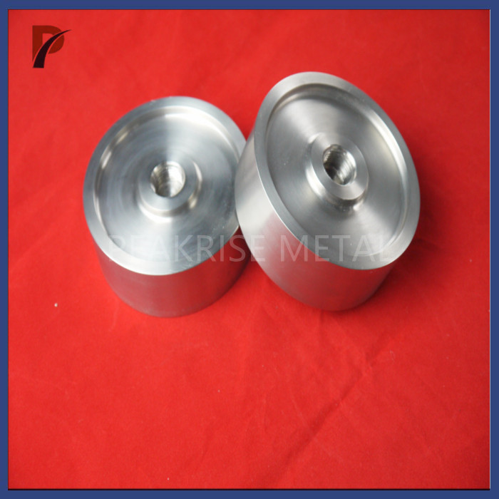
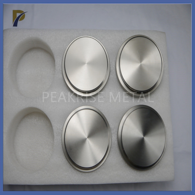
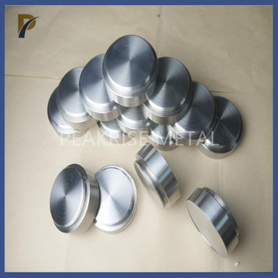
Molybdenum Sputtering Targets For The Semiconductor Industry
1. Description Of Molybdenum Sputtering Targets For The Semiconductor Industry:
Molybdenum is a versatile refractory metal with outstanding mechanical qualities, a low coefficient of expansion, strong thermal conductivity, and exceptionally high electrical conductivity at high temperatures. There are numerous combinations that can be used as sputtering targets, including pure molybdenum targets, molybdenum titanium targets, molybdenum tantalum targets, and molybdenum alloy targets (such as TZM plate).
The materials used for semiconductors include pure metal targets such as tungsten, molybdenum, niobium, titanium, and silicon, additionally to substances like oxides or nitrides. As crucial as the deposition operating parameters that engineers and scientists perfect throughout the coating process are the material selection procedure.
2. Size Of Molybdenum Sputtering Targets For The Semiconductor Industry:
Thickness : <20mm
Diameter: <300mm
Surface: Polished
Standard: ASTM B386
Other size can be processed according to customer's drawing.
![]()
![]()
3. Chemical Content Of Molybdenum Sputtering Targets For The Semiconductor Industry:
| Quantitative analysis | ||||||||||||||||||||||||||||||||||||||||||||||||||||||||||||
| Element | Ni | Mg | Fe | Pb | Al | Bi | Si | Cd | Ca | P | ||||||||||||||||||||||||||||||||||||||||||||||||||
| Concentration(%) | 0.003 | 0.002 | 0.005 | 0.0001 | 0.002 | 0.0001 | 0.002 | 0.0001 | 0.002 | 0.001 | ||||||||||||||||||||||||||||||||||||||||||||||||||
| Element | C | O | N | Sb | Sn | |||||||||||||||||||||||||||||||||||||||||||||||||||||||
| Concentration(%) | 0.01 | 0.003 | 0.003 | 0.0005 | 0.0001 | |||||||||||||||||||||||||||||||||||||||||||||||||||||||
| Purity(Metallic Base) Mo≥99.95% | ||||||||||||||||||||||||||||||||||||||||||||||||||||||||||||
|
||||||||||||||||||||||||||||||||||||||||||||||||||||||||||||
4. Physical and Mechanical Properties Of Molybdenum Sputtering Targets For The Semiconductor Industry:
| Properties | Pure Molybdenum | Doped Molybdenum | High temperature molybdenum alloy | ||
| Atomic coefficient | 42 | ||||
| Atomic weight(m) | 95.95 | ||||
| Lattice constant(a) | body centered cube | 3.14’10-10 | |||
| Density(r) | 10.2g/cm3 | ||||
| Melting point(t) | 2620±10℃ | ||||
| Boiling point(t) | 4800℃ | ||||
| Linear expansion coefficient(a1) | 20℃ | 5.3’10-6/K | 5.3’10-6/K | 5.3’10-6/K | |
| 20-1000℃ | 5.8’10-6/K | 5.8’10-6/K | 5.8’10-6/K | ||
| 20-1500℃ | 6.5’10-6/K | 6.5’10-6/K | 6.5’10-6/K | ||
| Specific heat(u) | 20℃ | 0.25J/g·K | 0.25J/g·K | 0.25J/g·K | |
| 1000℃ | 0.31J/g·K | 0.31J/g·K | 0.31J/g·K | ||
| 2000℃ | 0.44J/g·K | 0.44J/g·K | 0.44J/g·K | ||
| Thermal conductivity(l) | 20℃ | 142 W/m·K | 142 W/m·K | 126 W/m·K | |
| 1000℃ | 105 W/m·K | 105 W/m·K | 98 W/m·K | ||
| 1500℃ | 88 W/m·K | 88 W/m·K | 86 W/m·K | ||
| Resistivity(r) | 20℃ | 0.052mWm | 0.065mWm | 0.055mWm | |
| 1000℃ | 0.27mWm | 0.28mWm | 0.31mWm | ||
| 1500℃ | 0.43mWm | 0.43mWm | 0.45mWm | ||
| 2000℃ | 0.60mWm | 0.63mWm | 0.66mWm | ||
| Radiant energy | 730℃ | 5500.0W/m2 | |||
| 1330℃ | 6300.0W/m2 | ||||
| 1730℃ | 19200.0W/m2 | ||||
| 2330℃ | 700000.0W/m2 | ||||
| Thermal Neutron Absorption Cross Section | 2.7’10-28m2 | 2.7’10-28m2 | 2.7’10-28m2 | ||
| Tensile strength(Sb) | 0.10-8.00mm plate | 590~785MPa | 450~520MPa | 690~1130MPa | |
| f0.80 wire | 1020MPa | 1570MPa | |||
| Yield Strength(S0.2) | 0.10-8.00mm plate | 540~620MPa | 290~360MPa | 620~1000MPa | |
| Elongation(%) | 0.10-8.00mm plate | 3~17 | 15~75 | 2~8 | |
| f0.80 wire | 1.5 | 2 | |||
| Elastic Modulus(E) | 20℃ | 320GPa | 320GPa | 320GPa | |
| 1000℃ | 270GPa | 270GPa | 270GPa | ||
| Hardness(HV10) | <70% Deformation plate | 200~280 | 240~340 | ||
| >70% Deformation plate | 260~360 | 300~450 | |||
| Recrystallized plate | 140~160 | 170~190 | <200 | ||
| Plastic-brittle transition temperature(T) | -40~40℃ | ||||
| Initial recrystallization temperature(T) | >90%Deformation plate 1h Annealed | 900℃ | 1400℃ | 1250℃ | |
| final recrystallization temperature(T) | Annealed by 1 | 1200℃ | 1700℃ | 1600℃ | |
5. Features Of Molybdenum Sputtering Targets For The Semiconductor Industry:
The sputtered coating adheres to the substrate better than conventional deposition techniques, and materials with very high melting temperatures, like molybdenum and tungsten, are very simple to sputter. Additionally, whereas evaporation can only be done from bottom to top, sputtering can be done both ways.
Sputtering targets are frequently rounded or rectangular, although there are also square and triangular options available. The substrate is the item that needs to be coated, and it might be anything from solar cells to optical components to semiconductor wafers. The coating typically ranges in thickness from angstroms to microns. The membrane may consist of a single material or several materials stacked in layers.
High purity, high density, fine, and consistent grain properties are present in molybdenum sputtering targets, resulting in extremely high sputtering efficiency, homogeneous film thickness, and a clean etching surface throughout the sputtering process.

Please click below button for learn more our products.
![]()
![]()
Recommended Products